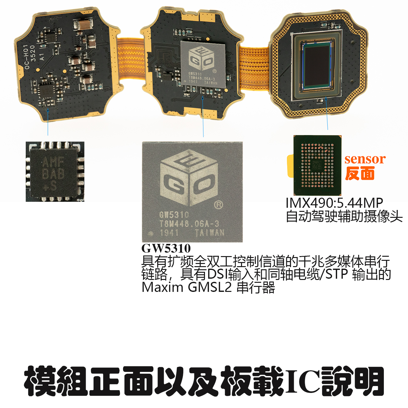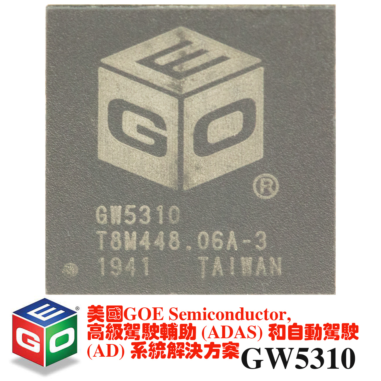
GW5300(GW5310)
GENERAL DESCRIPTION
The GW5300 is an advanced Camera Video Processor (CVP) System-on-Chip (SoC) designed for high-resolution sensor automotive applications. The GW5300 includes GEO’s proprietary 5th-generation eWARP? geometric processor, innovative High Dynamic Range (HDR) Image Signal processor (ISP), and 2D graphics functionality. Designed in a 28nm process to enable small, low power automotive cameras on-the-edge, the GW5300 supports ASIL B and AEC Q100 Grade 2.
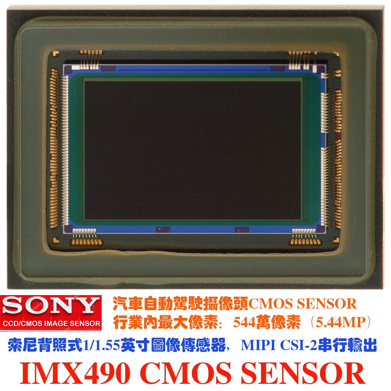
The HDR ISP supports up to 8MP30 or 5MP60, and LED Flicker Mitigation (LFM) techniques by pairing with the latest automotive sensors from On Semi, Sony, Omnivision, Samsung, Panasonic, and ST. GW5300’s on-chip combining of up to four exposures drives dynamic range up to 145dB. The 2D Vector Graphics Engine renders high resolution real-time graphics to overlay on the video stream enabling compelling user interfaces.
The GW5300 reduces system component count by requiring no external DDR memory and incorporating dual camera inputs. GW5300 based designs can be rapidly brought to market by leveraging GEO’s SDK and EVK.
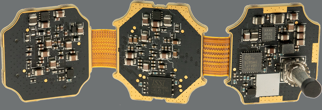
GW5300 BLOCK DIAGRAM
GW5200 Block Diagram
APPLICATIONS
. ADAS/AD Cameras
. Augmented Reality
. Videoconferencing
. DVR
FEATURES
eWARP? Geometric Processor
. 5th-gen eWARP? geometric processor
. Ultra-wide field of view (FOV) lens distortion correction
. Dynamic Electronic Pan/Tilt/Zoom (ePTZ)
. AutoCAL? digital calibration for extrinsic camera alignment
. Ultra-low latency (typically 1/6th of a frame)
HDR Image Signal Processor
. Supports up to 8MP30, 5MP60, or 12MP20 image sensors
. High Dynamic Range (HDR) processing
. Advanced spatial (2D) noise reduction
. Zone-based statistics for AE and AWB
. Dynamic defect and lens shading correction
. Color Noise Reduction, Purple Fringe Correction
. Defog support
Overlay Graphics
. Blending of up to 8 layers
. Fully independent alpha values across layers and pixels
. Vector Graphics Engine
On-the-fly rendering: 1920×1080 at 60fps
High quality multi-sampled anti-aliased rendering
. Pre-rendered bitmaps
Up to 4096×4096 bitmap resolution
256 colors selectable from 24bpp true color range per layer
In-line on-chip de-compression for memory savings
System Features
. CAN 2.0B, CAN FD, 3x I2C, 2x SPI, 2x UART, 15x GPIO, 3x PWM, JTAG, eFuse
I/O Interfaces
. Input: 2x MIPI CSI-2 4-lane @ 1.5Gbps/lane
. Output: 1x or 2x MIPI CSI-2 4-lane @1.5Gbps/lane
. Input: 16-bit parallel @ 150MHz
. Output: 16-bit parallel @ 150MHz
. Note: Parallel input and output not supported together
Automotive Safety
. ISO26262 Safety Element out of Context (SEooC) – ASIL B
. System health monitoring, status reporting, and Safe State
. ECC support for all processor code spaces
. Interface support for error detection and correction modes
. Embedded video and system statistics in output stream
. Voltage and temperature sensors, watch dog timer
Electrical Specifications
. Supply voltages:
Core: 0.9V ±5%
PLL and MIPI: 1.8V ±5%
I/O: 1.8V or 2.5V or 3.3V ±5%
. Power:
. Automotive: AEC Q100 Grade 2 (-40°C to 105°C)
. Industrial: -40°C to 85°C
Package
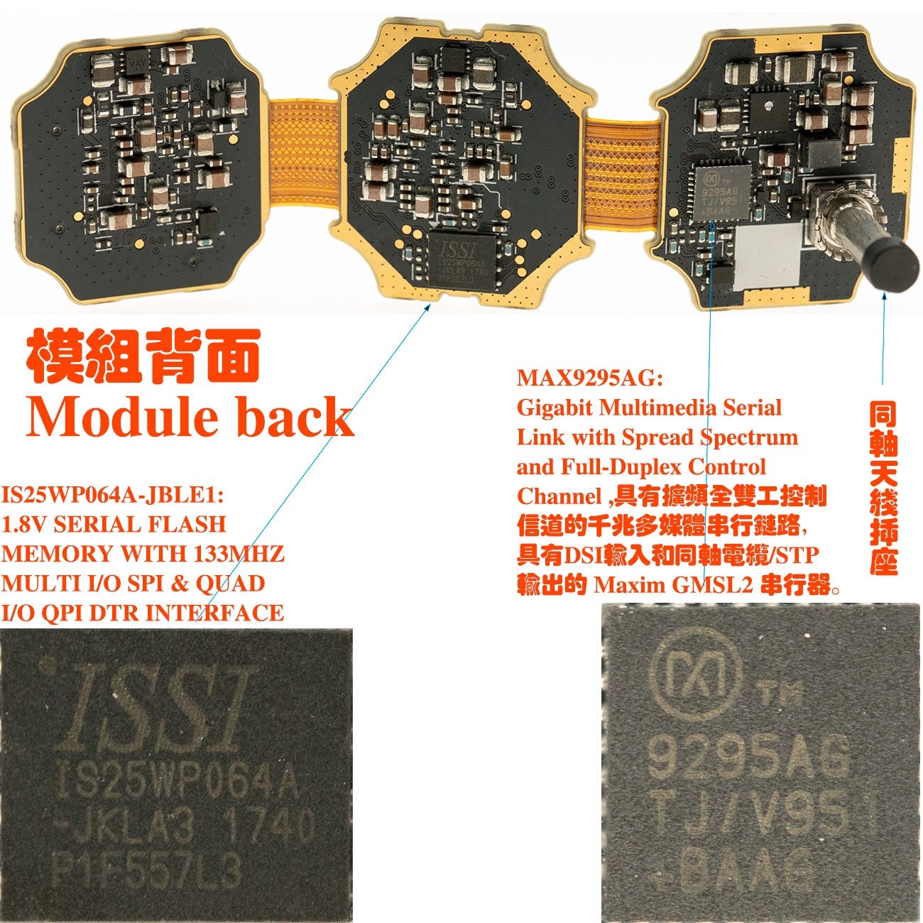
. 169-ball TFBGA 7mm x 7mm, 0.50mm pitch (GW5300 – 1x MIPI output)
. 196-ball TFBGA 10mm x 10mm, 0.65mm pitch (GW5310 – 2x MIPI output)
. RoHS/Lead-Free
GW5300 (GW5310)
一般的描述
GW5300是一款先进的摄像机视频处理器(CVP)片上系统(SoC),专为高分辨率传感器汽车应用而设计。GW5300包括GEO公司专有的第五代eWARP?几何处理器、创新的高动态范围(HDR)图像信号处理器(ISP)和2D图形功能。GW5300采用28nm工艺设计,支持ASIL B和AEC Q100 Grade 2,可以实现小型、低功耗的汽车摄像头。
HDR ISP通过与On Semi、Sony、Omnivision、Samsung、Panasonic和ST. GW5300的最新汽车传感器配对,支持高达8MP30或5MP60和LED闪烁缓解(LFM)技术,芯片上组合多达四种曝光驱动器的动态范围高达145dB。2D矢量图形引擎呈现高分辨率的实时图形,覆盖在视频流上,实现引人注目的用户界面。
GW5300不需要外部DDR内存和双摄像头输入,从而减少系统组件数量。通过利用GEO的SDK和EVK,基于GW5300的设计可以迅速推向市场。
GW5300框图
GW5200框图
应用
. ADAS /广告相机
. 增强现实
. 视频会议
. DVR
特性
eWARP?几何处理器
. 五代eWARP?几何处理器
. 超宽视场(FOV)镜头畸变校正
. 动态电子平移/倾斜/变焦(ePTZ)
. AutoCAL?数字校准外部相机校准
. 超低延迟(通常是1/6帧)
HDR图像信号处理器
. 支持8MP30、5MP60或12MP20图像传感器
. 高动态范围(HDR)处理
. 高级空间(2D)降噪
. 基于区域的AE和AWB统计
. 动态缺陷和镜头遮光校正
. 色彩噪声减少,紫色条纹校正
. 除雾的支持
叠加图形
. 混合多达8层
. 完全独立的alpha值跨越图层和像素
. 矢量图形引擎
*动态渲染:1920×1080, 60fps
*高质量的多采样抗锯齿渲染
. 预渲染位图
*高达4096×4096位图分辨率
*256色可选,每层24bpp真色范围
*内联片上解压缩,节省内存
系统功能
. CAN 2.0B, CAN FD, 3倍I2C, 2倍SPI, 2倍UART, 15倍GPIO, 3倍PWM, JTAG, fuse
I / O接口
. 输入:2x MIPI CSI-2 4 lane @ 1.5Gbps/lane
. 输出:1x或2x MIPI CSI-2 4 lane @1.5Gbps/lane
. 输入:16位并行@ 150MHz
. 输出:16位并行@ 150MHz
. 注:不支持并行输入和输出
汽车安全
. ISO26262安全组件脱离上下文(SEooC) - ASIL B
. 系统运行状况监视、状态报告和安全状态
. ECC支持所有处理器代码空间
. 接口支持错误检测和修正模式
. 嵌入式视频和系统统计输出流
. 电压和温度传感器,看门狗定时器
电气规格
. 供应电压:
*核心:0.9 v±5%
*锁相环和MIPI: 1.8V±5%
*I/O: 1.8V或2.5V或3.3V±5%
. 电源:
. 汽车:AEC Q100 2级(-40°C至105°C)
. 工业:-40°C至85°C
封装:
. 169球TFBGA 7mm x 7mm, 0.50mm间距(GW5300 - 1x MIPI输出)
. 196球TFBGA 10mm x 10mm, 0.65mm间距(GW5310 - 2x MIPI输出)
. RoHS /无铅
--------------------------------------------------------------------------------------------------------------------
GEO SEMI ANNOUNCES HIGH RESOLUTION ADAS AND AUTONOMOUS DRIVING SYSTEMS DESIGN WINS
GEO Semi Announces High Resolution ADAS and Autonomous Driving Systems Design Wins
The GW53x0 Product Provides High Resolution Solutions for Future ADAS and AD Automotive Systems
SAN JOSE, Calif. , July 28, 2020 GEO Semiconductor Inc. (“GEO”), the market leader in camera video processors (CVP) for automotive cameras, today announced new design wins for Autonomous and ADAS system applications using the GW53x0 product and supporting high resolution and HDR processing.
GEO’s application specific camera video processors include both the GW4 and GW5 product lines. These products feature world class high dynamic range image processing, geometric processing, featuring GEO’s eWARP? technology, overlay graphics, and in the case of the GW54x0, a DSP processor for computer vision processing.
Leveraging a versatile design architecture with a small package footprint, low power design, and low cost, without requiring an external DRAM memory, the GW4 and GW5 products stand out as a solution to a number of camera and video applications in the fast developing automotive market.
Today, GEO is engaged with multiple OEMs and industry processor partners for Advanced Driver Assistance (ADAS) and Autonomous Driving (AD) system solutions. For these applications GEO’s GW53x0 product supports high resolution (8 megapixel), high dynamic range automotive image sensors with unique Color Filter Array patterns such as RGGB, RCCB, and RYYCy. The GW53x0 enables customers to customize the image quality to support viewing outputs as well as optimizing the tuning to feed today’s Computer Vision processors for decision making in ADAS or AD applications.
“The GW53x0s high resolution HDR capability, ASIL B support, and the eWARP? processors ability to correct distortion and provide Region of Interest (ROI) selection make it an ideal processor for many ADAS applications,” said John Casey, GEO VP and GM for Automotive. “With design wins at traditional OEM’s, many of the emerging AD system and ride sharing companies, as well as solutions with multiple Autonomous Driving chip suppliers, GEO is well positioned to participate in the next generation ADAS and AD automotive application space.”
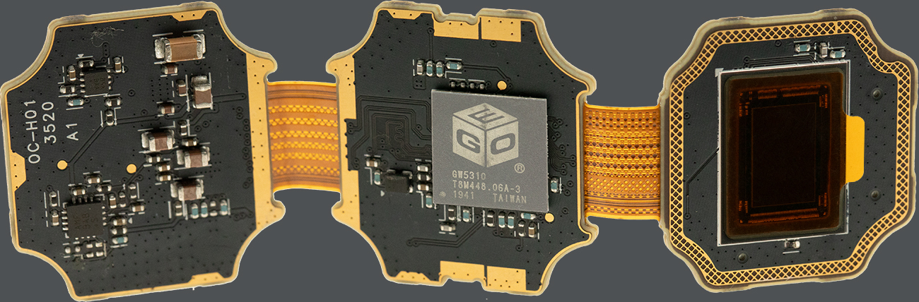
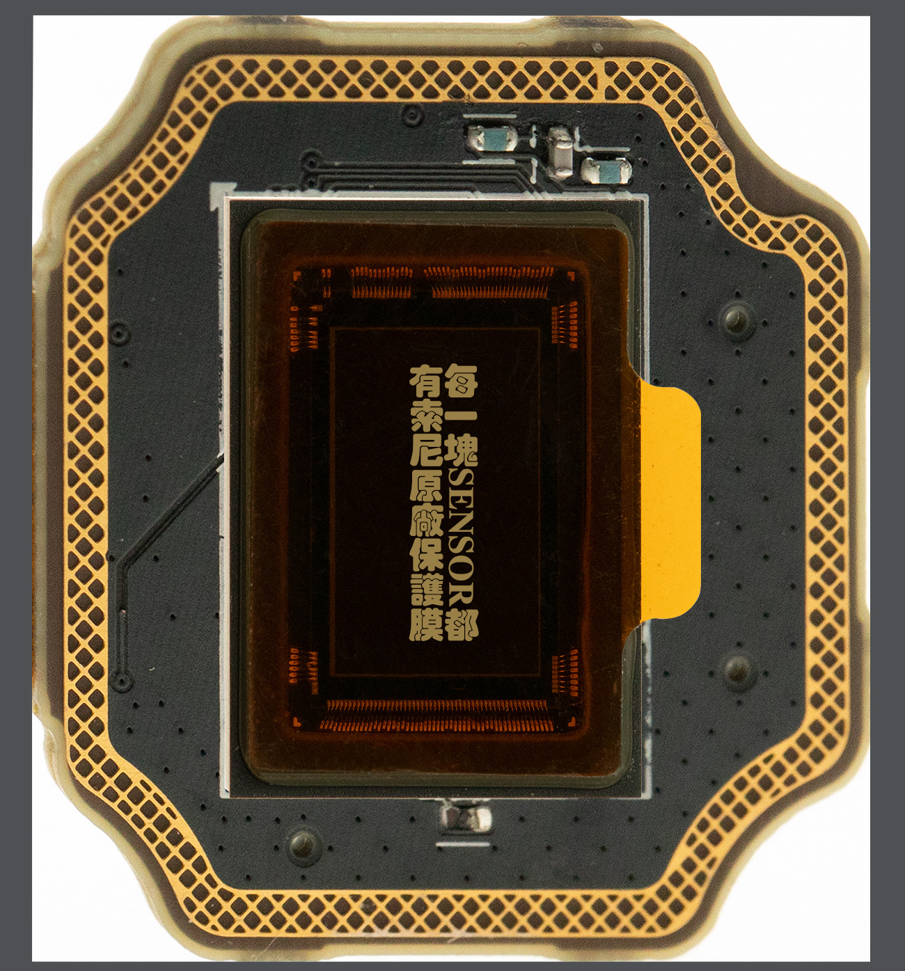
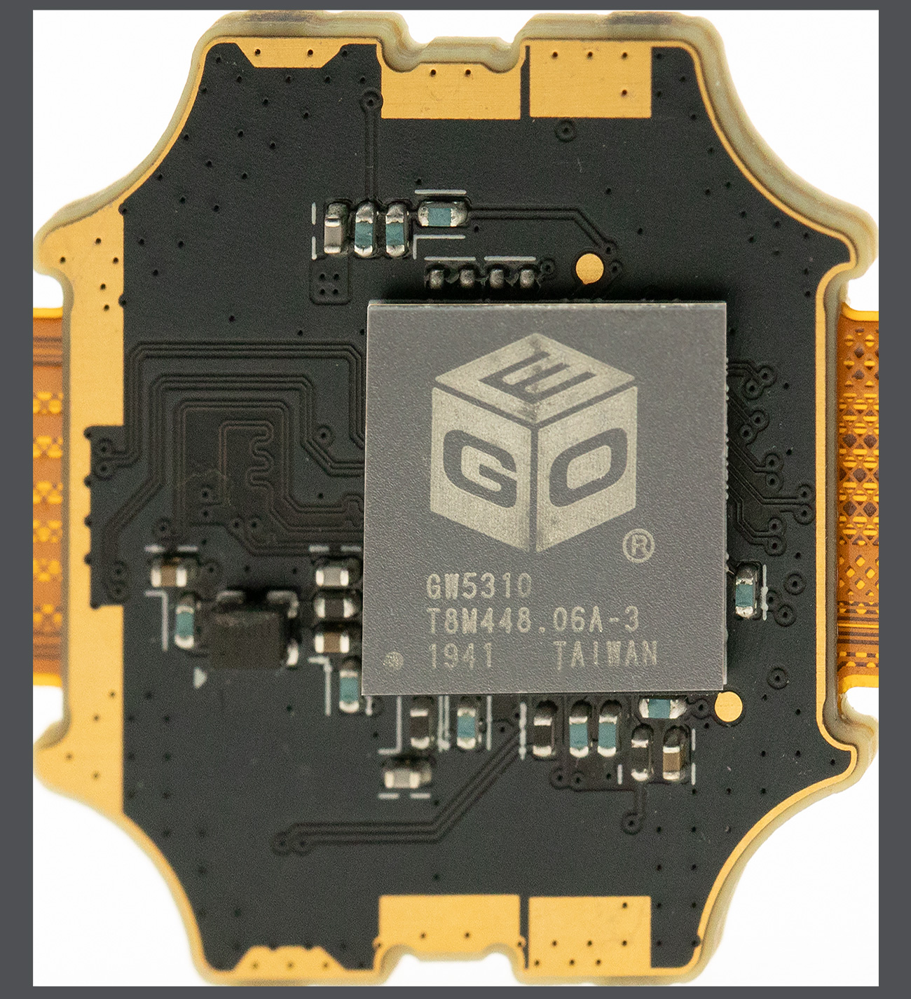
The GW53x0 is in Mass Production, supports up to 12 megapixel resolution, full HDR processing, and is capable of processing RGGB, RCCB, and RYYCy color filter sensor designs. The product supports integration into ASIL B systems, and simultaneously outputs a YUV color processed video stream while providing a RAW video stream over CSI-2 MIPI outputs. The GW5300 is available in 7mm x 7mm BGA package with 0.50mm ball pitch and the GW5310 is available in 10mm x 10mm BGA package with 0.65mm ball pitch.
About GEO Semiconductor
GEO Semiconductor Inc. is a private fabless semiconductor company developing camera video processors for automotive viewing and ADAS cameras. GEO’s value proposition is to provide automotive Tier-1s with the best products, tools, and support to guarantee exceptional image quality and system performance. GEO is headquarteredin San Jose, CA with global representation in the U.S., Canada, Europe, China, Japan, Korea, and Taiwan. The company is led by world-class imaging and video professionals with extensive experience in research, implementation, and optimization of image signal processing, geometric processing, and computer vision processing for embedded platforms.